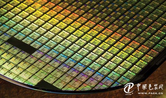
[Chinese Packaging Network News] Foundry foundry companies including TSMC, Intel, Samsung and other companies will gradually enter the process into 10 nanometers in 2017, and are ready to enter the 7nm process trial production in 2018, and even 2020 will Introduced 5nm process technology. Therefore, with the improvement of process technology, semiconductor manufacturing processes are increasingly approaching the limit, and manufacturing is increasingly difficult. As far as the process after 5 nanometers is concerned, there is no clear conclusion so far. In this regard, researchers at the Brookhaven National Laboratory (BNL) have announced that they have developed related technologies and equipment that can achieve a 1nm process.
According to foreign reports, researchers at the Brookhaven National Laboratory under the U.S. Department of Energy announced the successful use of electron beam printing technology to successfully manufacture printing equipment with a size of only 1 nanometer. It is understood that researchers in this laboratory use electron microscopy to produce smaller sizes than can be achieved with conventional electron beam printing (EBL) technology. This enables the electron-sensitive material to be greatly reduced in size under the effect of the focused electron beam, to the extent that a single atom can be manipulated. The birth of this technology and equipment can greatly change the material characteristics, from conduction to light transmission, or interactive execution in these two states.
As far as the content of the current publication is concerned, 1 nanometer printing uses a scanning projection electron microscope (STEM), separated by 11 nanometers, to achieve a density of 1 trillion features per square millimeter. The deviation correction STEM was used to achieve a resolution of 2 nm at a 5 nm half-gate under a hydroxide silicate resist.
Although this is not the first time that scientists have reached a nanometer level technology, another national laboratory under the US Department of Energy in 2016 also announced the development of a 1nm process technology. This section uses new materials such as carbon nanotubes and molybdenum disulfide. However, no matter which side is developing new technologies and equipment, it is currently observed that this technology will not be mass-produced soon. Because carbon nanotube transistors, like PMMA and electron beam lithography, are significantly different from current semiconductor process technologies. Therefore, it will take some time for the vendors to eliminate all existing equipment all at once.
Pet Clothes brands have become an indispensable part of the clothing industry. More and more people are adopting one or more pets. Every day they come home from get off work and see pets running to the door to greet them, the warmth is impossible. Speaking of words, the owners also like to see their little pets all dressed up and go out for a walk together. The pet clothing brand has also developed and grown with the love and affection of pet owners. We are a leading pet clothing, Pet Nightwear manufacturer and supplier in China, we specialize in Bathrobe For Dogs, Super Absorbent Pet Bathrobe and more.

Pet Clothes,Pet Nightwear,Bathrobe For Dogs,Super Absorbent Pet Bathrobe
Mianyang Crossing Cross-Border E-Commerce Co., Ltd. , https://www.wycypets.com